
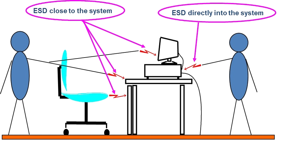
The below schematic gives a representation of possible causes of an IEC ( International Electrotechnical Comission) ESD event. Electrostatic charges accumulate on human bodies and furniture through triboelectric charging. A System Level ESD event is caused by a charged human discharging through a metallic tool such as a screw-driver directly into or adjacent to an electronic system, or a chair or piece of furniture adjacent to an electronic system discharging into the electronic system.
The system level ESD events could cause two types of failures in a system:
1: Soft failures or disturbances to the affected systems operation (e.g., reset, lock-up, loss of data).
2: Hard failures or catastrophic damage to the electronic components of the system.
/br>
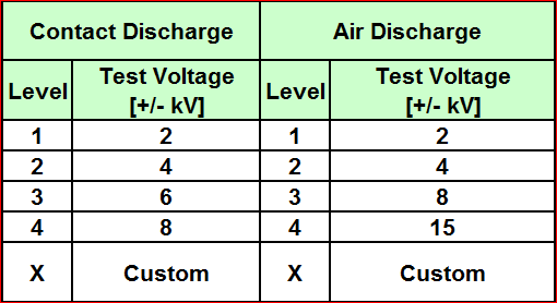
IEC stress testing is done on a isolated stress table as shown in schematic below. IEC stress testing companies as Keystone Compliance will take products and stress test them using IEC 61000-4-2 stress levels and procedures.
For further information on IEC voltages and IEC stress procedures see:

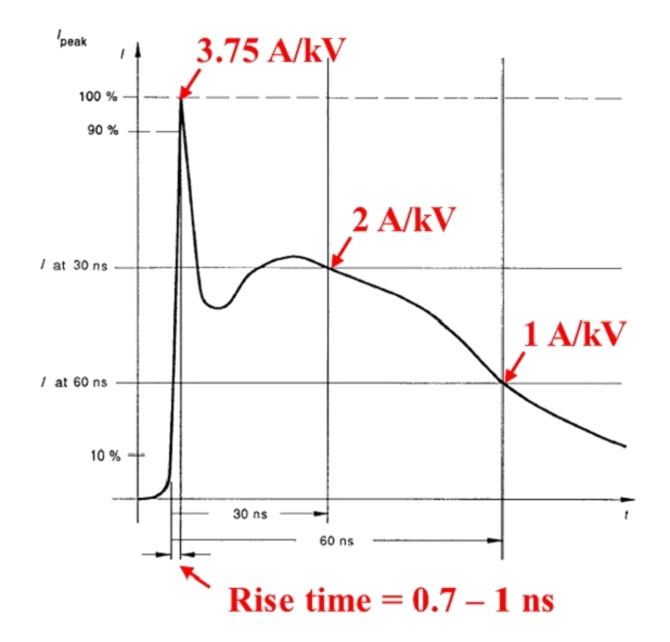
IEC stress standard defines two types of stress discharge modes, Contact discharge to simulate charged human touching electronic system and Air discharge to simulate arc discharge of a human or object to an electronic system. The IEC 61000-4-2 stress levels are given in the table at below left. The typical requirements are 4-8kv contact discharge and 8-15kv air discharge, however each company may have unique requirements. The waveform at below right gives the IEC stress current waveform at different stress voltage levels.
How To Solve System ESD Failures
1: System ESD stresses are applied to a system or a subsystem at the PCB (Printed Circuit Board) level or at the system or subsystem enclosure level while system or subsystem are powered up and operating in specified modes.
2: Contact stresses are applied to any metallized surface of the system or subsystem PCB (usually the PCB connectors) or system or subsystem enclosure. Air gap stresses are applied to any non-metallic surface of the system or subsystem PCB or enclosure.
3: System ESD failures are of two types:
A: Soft Failures: These types of failures are changes in system operation during or after a System ESD stress. These failures can be recovered after a system power down/up sequence or a system reset.
B: Hard Failures: These types of failures cause the system to alter its state permanently (the system does not recover to normal operation with a power down/up cycle or a system reset).
Key PCB Design Recommendations for Avoidance of System ESD failures
1: PCB soft or hard failures resulting from an applied System ESD stress are usually due to inadequate shunting of the applied System ESD stress pulse current to a low impedance PCB system ground plane.
2: During a System ESD stress, significant disturbances occur in the PCB ground or supply planes if these are not adequatly decoupled.
3: It is good practice to have the top layer of the PCB as the signal layer and the 2nd PCB layer a very low impedance PCB system ground layer. Any via's which connect a ground connection on the signal layer to the second PCB ground layer have to be very low impedance to allows for low resistance shunting of the applied ESD stress current to the low impedance ground plane.
A: With a low impedance second layer ground plane and very low resistance via's to this ground plane, any IEC ESD stresses applied to a PCB connector enclosure will be efficiently shunted to the pcb ground plane at the connector.
B: Any IEC ESD stress current caught by Transient Voltage Suppressor (TVS) diodes will be shunted to the low impedance PCB ground plane before they can cause damage to integrated circuit pins.
4: It is good practice to decouple any high impedance PCB integrated circuit traces which are inputs to integrated circuits and can asynchronously modify system operation, using a series of filtering capacitors placed as close as possible to the integrated circuit package on the PCB.
5: It is good practice to place all clock circuits as close as possible to the integrated circuit with clock pins traversing shielded by second layer PCB ground plane to the integrated circuit pins. Alternatively, buffer the clock pins close the clock circuit before routing to integrated circuit pins.
6: MOST PCB traces connected directly from enclosure connector pins to an integrated circuit on the pcb must be protected with TVS (Transient Voltage Suppressor) diodes as close as possible to the enclosure connector. Sometimes, common mode chokes must be placed between TVS and integrated circuit for additional protection.
7: More information about IEC stress voltages and IEC stress procedures is given at:
Link to other ESD and Latch Up topics:
- Human Body Model (HBM) Charged Device Model (CDM) Machine Model (MM) Electrical Fast Transients (EFT)/Burst - IEC 61000-4-4 Lightning/Surge - IEC 61000-4-5 Automotive ESD - AEC Q100 and ISO 10605 Latch-Up Electrical Overstress (EOS) ESD and Latch Up Testing and Qualification Procedures
For immediate consulting help on the above topics, contact (blog with) ESD Unlimited LLC staff at the
Current local date and time in Alpine, Texas (United States)
Visitors Since June 16, 2019: