
This page of the ESD Unlimited LLC website discusses the details of ESD and Latch-Up Stress Testing and Qualification
- Click here to view the Human Body Model (HBM) ESD details section. Click here to view the Charged Device Model (CDM) ESD details section. Click here to view the Latch-Up (LU) details section. Click here to view the Machine Model (MM) ESD details section. Click here to view the System Level ESD details section. Click here to view the Electrical Fast Transient/Burst ESD details section. Click here to view the Lightning/Surge ESD details section. Click here to view the Stress Simulation / Qualification Companies and Requirements details section.
Human Body Model (HBM) Stress Simulation and Qualification
There are two HBM stress simulation methodologies. The first one is for non-automotive products and the second one is for automotive products.
Highlights of JEDEC HBM stress simulation methodology for non-automotive products
The stress simulation methodology for non-automotive products is describes in the document ANSI/ESDA/JEDEC JS 001-2014 which can be found at the JEDEC WEBSITE.
1: A minimum of three units are required for HBM stress simulations, at least one positive and one negative stress pulses need to be applied to all units under stress, three new samples for different polarities may be used. A unique set of 3 units for stress may be used for seperate stress combinations, stress levels, or device pins subsets to avoid the effects of cummulative stress.
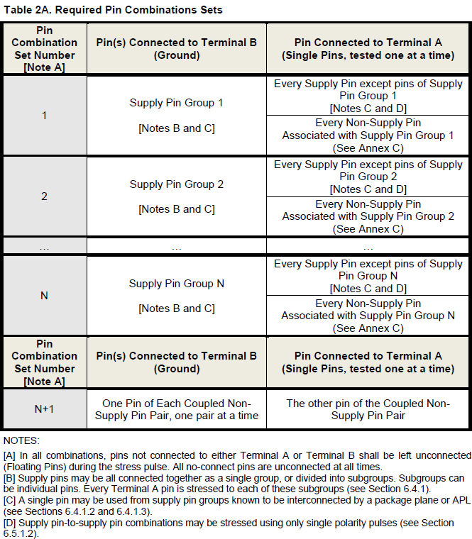
2: Pins are categorized as supply, non-supply, direct coupled no-supply pairs and no-connects and are stressed accordingly.
3: If a group of supply pins are connected via a package plane (or connected by an above passivation layer), one pin of that supply group may be used to represent this supply group and stressed, any other supply pin of this group does not need to be stressed and can be left floating during the stress tests. Similar condition holds true for shorted non-supply pins.
4: Verified no-connect pins do not need to be stressed. Pins are not no-connect if they have a low impedance connection to the die under test.
5:Non-supply pins are only stressed against a supply group they are associated with, if this information is not known, then every non-supply pin has to be stressed to each supply pin group.
6: When stressing supply pin groups to other supply pin groups stresses may be performed with single polarity only. For most technologies, such as CMOS circuits on p substrates, positive only testing is preferred. It has been observed that for CMOS circuits power supply stress with a negative polarity causes stress waveform distortions due to stress tester parasitics.
7: When stressing non-supply pins to supply pins negatively, stress tester parasitics impact the slew rate for the HBM pulse waveform. It is allowed to reconfigure this stress matrix to stressing each supply pin to each non-supply pin positively.
8: Same non-supply I-O pins (with the same on die IO topology) may be designated as Cloned and thus removed from the stress matrix.
9: The required stress pin combination sets during the simulation can be seen at below left and right. The purpose of the pin combinations is to test all of the major HBM current paths. Setting up the pin combinations requires knowledge of the device under test. Each pin of the device must be classified as a no connect, supply pin or non-supply pin, supply pins must be grouped into supply pin groups.The table on the below left Table 2a lists the preferred set of pin combinations required for device qualification. Alternatively the table on the right Table 2b can also be used this set of pin combination was specified in ANSI/ESDA/JEDEC JS-001-2010. However it is allowed to used pin stress combinations from the table on the below left and right to populate the device stress combination for qualification, documentation outlining the details of the stress combinations needs to be provided so that the stress procedure can be reproduced.

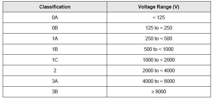
10: Recommended stress simulation levels have been determined to be +/-500v and +/-1000v. These levels have been deemed sufficient for HBM Qualification with typical manufacturing ESD controls installed. The below picture shows a full list of stress simulation levels categorized as HBM ESD Component Classification Levels any of the Classification levels other than for +/-500v and +/-1000v are for information only:

Back to Beginning of JEDEC HBM Discussion
Highlights of AEC Q100 HBM stress simulation methodology for automotive products
The stress simulation methodology for automotive products is describes in the document AEC-Q100-002-REV-E August 20, 2013 which can be found at the AEC Q100 WEBSITE.
The AEC-Q100 HBM stress test procedure is based on the HBM document ANSI/ESDA/JEDEC JS 001-2014, Q100 AEC HBM stressing is done in accordance with the ANSI/ESDA/JEDEC JS001 stress specification, however, there are notable exceptions as described in sections 1-3 below:
1: Use Table 2b for AEC Q100 HBM Qualification, if stress tester artifacts or cummulative stress is found to be the cause of the HBM stress failures use the options contained in Table 2a .
2: Upon completion of the required testing a report of the testing performed and detailed results including any deviations, shall be submitted to the customer upon request.
3: Stress simulation must be done and qualified at the following stress voltages: +/-500v, +/-1000v, and +/-2000v, voltage levels above +/-2000v may be done for margin, or high robustness characterization with the Component Classification Levels remaining the same.
Back to top of this pageCharged Device Model (CDM) Stress Simulation and Qualification
There are two CDM stress simulation methodologies. The first one is for non-automotive products and the second one is for automotive products.
Highlights of JEDEC CDM stress simulation methodology for non-automotive products
This ESD stress simulation model is described in document ANSI/ESDA/JEDEC JS 002-2014 and is available at JEDEC WEBSITE.
1: A minimum of three units are required for this stress simulation. Each pin of an integrated circuit is stressed once positive and once negative during the full CDM simulation.
2: For each device, apply at least one positive and one negative discharge to each pin. Stresses may be partitioned by polarity, using a sample size of at least three units per polarity. Pins may also be partitioned into one or more sets of samples, provided that each pin of the device is a member of at least one set. Each set shall have a minimum of three units.
3: The recommended stress simulation level has been determined to be +/-250v. This level has been deemed sufficient for CDM Qualification with typical manufacturing ESD controls installed. The below picture shows a full list of stress simulation levels categorized as CDM ESD Component Classification Levels, voltage levels above +/-250v may be done for margin, or high robustness characterization with the Component Classification Level remaining the same.
Back to Beginning of JEDEC HBM Discussion
Highlights of AEC Q100 CDM stress simulation methodology for automotive products
This ESD stress simulation model is described in document AEC - Q100-011 - REV-C1 March 12, 2013 and is available at AEC Q100 WEBSITE.
1: A minimum of three units are required for this stress simulation. Each pin of an integrated circuit is stressed three times at same voltage positive and negative during the full CDM simulation. Pin subsets of the integrated circuits may be stressed individually as long as at least 3 units to stress for each subset is made available and each pin is stressed three times positive and three times negative.
2: Upon completion of the required stress testing, a report of the testing performed and detailed results, including any deviations, shall be submitted to the stress evaluation requestor upon request.
3: The required stress simulation levels are +/-250v and +/-500v. Corner pins (balls) are stressed to +/-750v The below picture shows a full list of stress simulation levels categorized as CDM ESD Component Classification Levels:
 Back to top of this page
Latch-Up Stress Simulation and Qualification
There are two Latch-Up stress simulation methodologies. The first one is for non-automotive products and the second one is for automotive products.
Highlights of JEDEC Latch-Up stress simulation methodology for non-automotive products
This Latch-Up simulation model is described in document JESD78E April 2016 and is available at JEDEC WEBSITE.
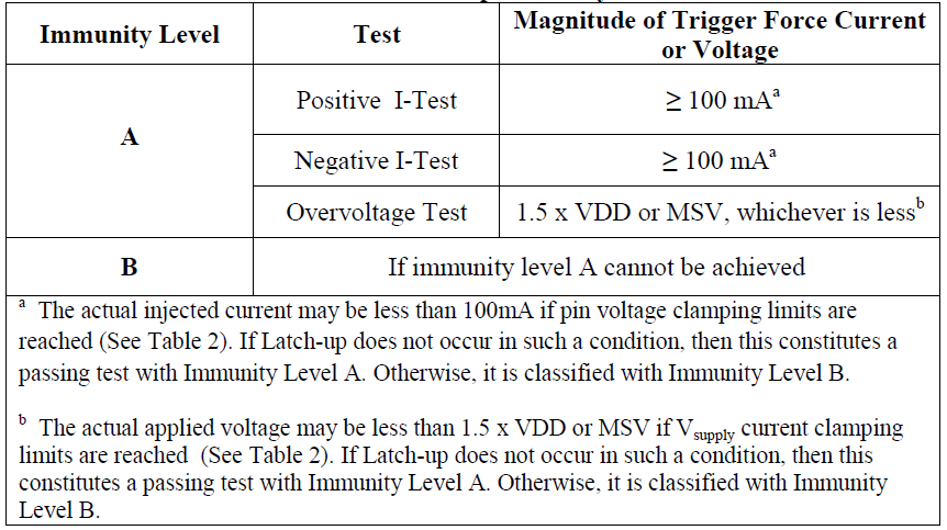
1: Integrated circuit Latch-Up immunity is characterized via current injection to the device pins and an overvoltage to the device under test power pins. The below table outlines the stress current and voltage levels for the Latch-Up stress test:
2: There are two classes for Latch-Up testing. Class I is stress testing integrated circuit at room temperature ambient. Class II is stress testing the integrated circuits at the maximum operating ambient temperature (Ta) or maximum operating case temperature (Tc) or maximum operating junction temperature of the integrated circuit in the data sheet. (Ta, Tc, or Tj) should be selected to duplicate the temperature characteristic of the integrated circuit during operation as indicated in the data sheet.
3: The integrated circuit under Latch-Up test must be preconditioned in such a manner that any Inputs/Outputs are placed in a HIZ state, and any external applied levels on Input only pins must not affect the state of the integrated circuit during the Latch-Up stress procedure when a stress HI or LO level is applied to them. If any input pins must be in a defined state to avoid violating preconditioning requirements of the integrated circuit, the pin can only be stressed in its defined state.
4: During the current trigger method of the functional pin Latch-Up stress test the funtional pin voltage is clamped to 1.5x of the interacting Vmaxsupply for positive current injection (and -0.5x of the Interacting Vmaxsupply for negative current injection) and at the same time the pin is clamped to >=100ma for positive current injection (and <=-100ma for negative current injection). Pin failure occurs (pin latches up) when the pin injection trigger current is removed and any supply of the integrated circuit is greater than or equal to 1.4x the I nom current of the supply.
5: Supply group Latch-Up stress occurs when supply is raised to 1.5x Vmax of the supply. Supply failure (supply latches up) when supply voltage is reduced to Vmax and supply current is greater than or equal to 1.4x I nom current of the supply.
Back to Beginning of JEDEC Latch-Up Discussion
Highlights of AEC Q100 Latch-Up stress simulation methodology for automotive products
This ESD stress simulation model is described in document AEC - Q100-004 - REV-D August 7, 2012 and is available at AEC Q100 WEBSITE.
This Latch-Up simulation procedure is conducted the same way as the Latch-Up simulation for latest revision of JESD78E April 2016 but contains several differences which are described below.1: Latch-Up stress qualification testing is to be performed with the integrated circuit under test at its maximum ambient operating temperatures as indicated in the integrated circuits specification.
2: Latch-Up stress simulation is allowed to be done using voltage trigger.
Back to top of this pageMachine Model (MM) Stress Simulation and Qualification
Due to higher accuracy of the CDM and HBM ESD stress simulation models, the MM is no longer a supported stress simulation model. Some customers may continue to require this model to be executed on integrated circuits. If so required, this simulation model should be executed in same way as the JEDEC HBM or AEC Q100 HBM AEC Q100 HBM simulation model with stress voltages to be adjusted as follows: Vhbm = 2kv => Vmm = 100v, and Vhbm = 1kv => Vmm=50v.
Back to top of this page
System Level ESD Stress Simulation and Qualification
There are two System ESD stress simulation methodologies. The first one is for non-automotive products and the second one is for automotive products.
Highlights of IEC System ESD stress simulation methodology for non-automotive products
The details for IEC System ESD concept and procedures are given atIEC System ESD.
1: A complete working system (pcb only or pcb +enclosure) and software for this system are required for this test. Any metalized surfaces on the working system enclosure (pcb) will receive direct stress and any non-conductive surfaces on the working system enclosure (pcb) will receive air gap stress. 2: Stresses will be applied to the external surfaces of the pcb enclosure, to metallized connectors of the pcb or enclosure (i.e. hdmi, usb, ethernet, etc connectors), to keyboard and display surfaces and to the vertical and/or horizontal coupling planes on which the enclosure or pcb under test resides.
3: Unless customer requires different, typical passing stress levels for contact discharge is +/-8kv and for air discharge is +/-15kv. 4: Unless customer requires different, at each stress polarity voltage level, 10 single discharges separated by 1 sec are recommended to be applied to the system under test.
5: It is sufficient to stress test one pcb board or system enclosure containing the pcb.
6: Further details on test set up and stress procedure can be found in the IEC System ESD 61000-4-2:2008 specification which can be bought at the IEC WEBSITE
Back to the beginning of the IEC System ESD Discussion
Highlights of AEC ISO System ESD stress simulation methodology for automotive products
AEC ISO System ESD concept and stress procedures are given at AEC ISO System ESD.
1: This System ESD stress specification covers the simulation of System ESD events during automobile assembly, System ESD events caused by automotive service staff and System ESD events caused by automotive occupants. The stress methodology is similar to the stress methodology for IEC 61000-4-2:2008 except that pcb and enclosure systems to be tested must be tested while operating (powered up) and not operating (not powered up), ISO uses different capacitance/resistance values to develop the stress pulse, and any communication ports (AV, USB, HDMI, Ethernet) must be stressed at the connector and at the far end of 1.7m communication cable.
2: Further details on test set up and stress procedure can be found in the IEC System ESD 61000-4-2:2008 spec which can be bought at the: ISO WEBSITE
Back to top of this page
Electrical Fast Transients (EFT)/Burst IEC 61000-4-4 Simulation and Qualification
Electrical Fast Transients (EFT) / Burst concept and stress procedures are given at IEC EFT / Burst at THIS WEBSITE
1: Further details on test set up and stress procedure can be found in the IEC EFT / Burst 61000-4-4:2012 RLV spec which can be bought: IEC WEBSITE
2: The stress methodology is similar to the stress methodology for IEC 61000-4-2:2008 except that the repetitive fast transient test is a test with bursts consisting of a number of fast transients, coupled into power supply, control and signal ports of electrical and electronic equipment. Significant for the test are the short rise time, the repetition rate and the low energy of the transients. Test voltages of up to 4 kV in positive and negative polarities are applied to the A/C power leads and up to 2 kV is applied to the I/O cables. The test voltages are at a 5 kHz pulse repetition frequency and applied for 60 seconds to each power supply terminal including protective earth and every combination of these terminals. The coupling clamp is used to apply up to 2 kV to the I/O cables.
Back to top of this page
Lightning / Surge IEC 61000-4-5:2014 Simulation and Qualification
Details for Lightning / Surge concept and procedures are given at IEC Lightning / Surge at THIS WEBSITE
1: Further details on test set up and stress procedure can be found in the Lightning / Surge 61000-4-5:2014 spec which can be bought: IEC WEBSITE
2: These tests relate to the immunity requirements for equipment to unidirectional surges caused by over voltages from switching and lightning transients. The surge is to be applied to the system under test power supply terminals via a captive coupling network.
Back to top of this page
Stress Simulation / Qualification Companies and Requirements
Stress simulation companies for HBM, MM, CDM, Latch Up
Innovative Circuits Engineering, Inc. provides Stress simulations for HBM, MM, CDM and Latch-Up. Company requires socketed pcb with all of the pins available at pcb card edge for the integrated circuit to be stress tested. Requires preconditioning test vectors to be applied to integrated circuit prior to Latch Up stress application. Requires information on how common supplies are ganged, the number and values of the stress voltages, the number of stress pulse to be applied to each pin for the same stress voltage, the polarity of stress pulses, and which of the pins are no connect, signal, and power pins.
Stress simulation companies for IEC 61000-4-2, -4-4, -4-5 stresses
ATLAS COMPLIANCE & ENGINEERING provides Stress simulations for IEC 61000-4-2, -4-4, -4-5. The following items need to be provided to initiate stress simulation work: User I/O ports, power requirements, clock frequencies, special facilities requirements, and sales brochure or product specification. Operating instructions and support equipment required. Performance criteria for evaluating stress tests.
Stress simulation companies for AEC Q100 HBM, MM, CDM and Latch-Up stresses
Innovative Circuits Engineering, Inc. provides stress simulations for AEC Q100 HBM, MM, CDM and Latch Up stress simulations.
Stress simulation companies for AEC ISO 10605:2008 stresses
ATLAS COMPLIANCE & ENGINEERING provides stress simulations for ISO 10605:2008.
Back to top of this page
Links to other ESD and Latch Up topics
- Human Body Model (HBM) Charged Device Model (CDM) Machine Model (MM) System Level ESD - IEC 61000-4-2 Electrical Fast Transients (EFT)/Burst - IEC 61000-4-4 Lightning/Surge - IEC 61000-4-5 Automotive ESD - AEC Q100 and ISO 10605 Latch-Up Electrical Overstress (EOS)
For immediate consulting help on the above topics, contact (blog with) ESD Unlimited LLC staff at the
Current local date and time in Alpine, Texas (United States)
Visitors Since June 16, 2019: